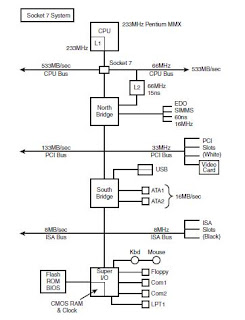
Processor socket architecture
Low insertion force (LIF)
Low insertion force (LIF) is a technology used in integrated circuit sockets that are designed so the force
required to insert or remove a package is low.
Initially,
the LIF connectors were designed as a cheaper alternative compared to zero insertion force (ZIF) connectors, to facilitate
programming and testing of equipment. Compared with standard IC sockets, they
have a lower friction force between the contacts of the device and the socket,
making insertion and removal of the device easier, while at the same time
eliminating the need for the complex mechanism that is used in ZIF sockets.
The
disadvantages of LIF connectors are that the grip force between the contacts is
lower, and the contacts can oxidize faster and decrease the lifespan of the
connector. With the advent of frequent changes in PC processors, a need arose
for these systems. Intel introduced the LIF socket system, in which the
processor is inserted into the socket, rather than fixed by a lever. This type
of socket was used for some types of 386s and early 486s. This type of socket
has been replaced by the ZIF socket, although LIF sockets are now used in
modern 1.8" hard disks.
Zero insertion force (ZIF) is a type of IC
socket or electrical connector that requires very little force for insertion.
With a ZIF socket, before the IC is inserted, a lever or slider on the side of
the socket is moved, pushing all the sprung contacts apart so that the IC can
be inserted with very little force - generally the weight of the IC itself is
sufficient and no external downward force is required. The lever is then moved
back, allowing the contacts to close and grip the pins of the IC. ZIF sockets
are much more expensive than standard IC sockets and also tend to take up a
larger board area due to the space taken up by the lever mechanism.
A dual in-line package (DIP or DIL), or
dual in-line pin package (DIPP) is an electronic component
package with a rectangular housing and two parallel rows of electrical connecting
pins. The package may be through-hole mounted to a printed circuit board or
inserted in a socket. DIPs can be mounted either by through-hole soldering or
in sockets. Sockets allow easy replacement of a device and eliminates the risk
of damage from overheating during soldering. Generally sockets were used for
high-value or large ICs, which cost much more than the socket.
Variants
Several DIP variants for ICs exist,
mostly distinguished by packaging material:
- Ceramic Dual In-line Package (CERDIP or CDIP)
- Plastic Dual In-line Package (PDIP)
- Shrink Plastic Dual In-line Package (SPDIP)
- Skinny Dual In-line Package (SDIP or SPDIP)
An SMT component is usually smaller than its through-hole counterpart because it has either smaller leads or no leads at all. It may have short pins or leads of various styles, flat contacts, a matrix of solder balls (BGAs), or terminations on the body of the component.
Advantages
The main advantages of SMT over the older through-hole technique are:- Smaller components. As of 2012 smallest was 0.4 × 0.2 mm (0.016 × 0.008 in: 01005). Expected to sample in 2013 are 0.25 × 0.125 mm (0.010 × 0.005 in, size not yet standardized)
- Much higher component density (components per unit area) and many more connections per component.
- Lower initial cost and time of setting up for production.
- Fewer holes need to be drilled.
- Simpler and faster automated assembly. Some placement machines are capable of placing more than 136,000 components per hour.
- Small errors in component placement are corrected automatically as the surface tension of molten solder pulls components into alignment with solder pads.
- Components can be placed on both sides of the circuit board.
- Lower resistance and inductance at the connection; consequently, fewer unwanted RF signal effects and better and more predictable high-frequency performance.
- Better mechanical performance under shake and vibration conditions.
- Many SMT parts cost less than equivalent through-hole parts.
- Better EMC performance (lower radiated emissions) due to the smaller radiation loop area (because of the smaller package) and the smaller lead inductance.
Disadvantages
- Manual prototype assembly or component-level repair is more difficult and requires skilled operators and more expensive tools, due to the small sizes and lead spacings of many SMDs.
- SMDs cannot be used directly with plug-in breadboards (a quick snap-and-play prototyping tool), requiring either a custom PCB for every prototype or the mounting of the SMD upon a pin-leaded carrier. For prototyping around a specific SMD component, a less-expensive breakout board may be used. Additionally, stripboard style protoboards can be used, some of which include pads for standard sized SMD components. For prototyping, "dead bug" breadboarding can be used.
- SMDs' solder connections may be damaged by potting compounds going through thermal cycling.
- Solder joint dimensions in SMT quickly become much smaller as advances are made toward ultra-fine pitch technology. The reliability of solder joints becomes more of a concern, as less and less solder is allowed for each joint. Voiding is a fault commonly associated with solder joints, especially when reflowing a solder paste in the SMT application. The presence of voids can deteriorate the joint strength and eventually lead to joint failure.
- SMT is unsuitable for large, high-power, or high-voltage parts, for example in power circuitry. It is common to combine SMT and through-hole construction, with transformers, heat-sinked power semiconductors, physically large capacitors, fuses, connectors, and so on mounted on one side of the PCB through holes.
- SMT is unsuitable as the sole attachment method for components that are subject to frequent mechanical stress, such as connectors that are used to interface with external devices that are frequently attached and detached.


Comments
Post a Comment